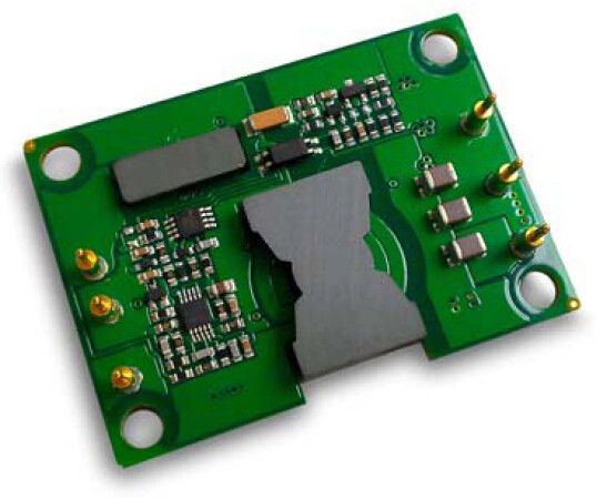
DC-DC Converters 40W Output 5V 8A XD40-24S5-POCW
Key Features
Output power: 40W
Wide input range: 20-60Vdc
High conversion efficiency: Up to 91%
Line regulation to ±1%
Load regulation to ±1%
Fixed operating frequency
Isolation voltage :1500V
Enable (ON/OFF) control
Output over-voltage protection
Output over-load protection
Hiccup mode short circuit protection
Over-temperature protection
Input under-voltage lock-out
Output voltage trim: -8~+10%
Product Overview
These DC-DC converter modules use advanced power
processing, control and packaging technologies to provide
the performance, flexibility, reliability and cost effectiveness
of a mature power component. High frequency Active Clamp
switching provides high power density with low noise and
high efficiency.
1. Electric Characteristics
Electrical characteristics apply over the full operating range of input voltage, output load and base plate temperature,unless otherwise specified. All temperatures refer to the operating temperature at the center of the base plate. All data testing at Ta=25oC except especial definition.
1.1 Absolute Maximum Ratings
|
Parameter
|
Min
|
Typ
|
Max
|
Units
|
Notes
|
|
Input Voltage
|
|
|
65
|
Vdc
|
Continuous, non-operating
|
|
|
|
60
|
Vdc
|
Continuous, operating
|
|
|
|
65
|
Vdc
|
Operating transient protection,<100mS
|
|
Isolation voltage
|
|
|
2000
|
Vdc
|
Input to output
|
|
Operating Temperature
|
-55
|
|
100
|
℃
|
|
|
Storage Temperature
|
-55
|
|
125
|
℃
|
|
|
Enable to -Vin Voltage
|
-2.0
|
|
10
|
Vdc
|
|
1.2 Input Characteristics
|
Parameter
|
Min
|
Typ
|
Max
|
Units
|
Notes
|
|
input voltage range
|
20
|
48
|
60
|
Vdc
|
Continuous
|
|
Under-Voltage Lockout
|
19.0
|
19.5
|
19.9
|
Vdc
|
Turn - On Threshold
|
|
18.0
|
18.5
|
19.0
|
Vdc
|
Turn - Off Threshold
|
|
Maximum Input Current
|
|
|
2.5
|
A
|
Full load;20Vdc Input
|
|
Efficiency
|
|
89
|
|
%
|
Figures 1-4
|
|
Dissipation
|
|
|
5
|
W
|
No load
|
|
Disabled Input Current
|
|
|
5
|
mA
|
Enable pin low
|
|
Recommend External Input
Capacitance
|
|
100
|
|
uF
|
Typical ESR 0.1-0.2W
|
1.3 Output Characteristics
|
Parameter
|
Min
|
Typ
|
Max
|
Units
|
Notes
|
|
Output Voltage Set point
|
4.95
|
5.00
|
5.05
|
Vdc
|
Nominal input; No load
|
|
Output Voltage Range
|
4.90
|
5.00
|
5.10
|
Vdc
|
No load to max load
|
|
Output Current Range
|
0
|
|
8
|
A
|
Subject to thermal derating, 100LFM,
Figures 5 - 8
|
|
Line Regulation
|
|
±0.2
|
±1
|
%
|
Low line to high line; full load
|
|
Load Regulation
|
|
±0.2
|
±1
|
%
|
No load to full load; nominal input
|
|
Temperature Regulation
|
|
±0.002
|
±0.02
|
% / °C
|
Over operating temperature range
|
|
Current limit
|
|
11
|
|
A
|
Output voltage 90% of nominal
|
|
Short circuit current
|
0
|
10
|
20
|
A
|
Output voltage <250 mV
|
|
Ripple (RMS)
|
|
15
|
|
mV
|
Nominal input; full load; 20 MHz
bandwidth; See Figure 13
|
|
Noise(Peak-to-Peak)
|
|
75
|
|
mV
|
|
Maximum Output Cap.
|
|
|
2200
|
μF
|
Nominal input; full load
|
|
Output Voltage Trim
|
-8
|
|
+10
|
%
|
Nominal input; full load
|
1.4 Dynamic Response Characteristics
|
Parameter
|
Min
|
Typ
|
Max
|
Units
|
Notes
|
|
Change in Output Current
(di/dt= 0.1A/us)
|
|
250
|
|
mV
|
50% to 75% to 50% Iout max; Figure 11
|
|
Change in Output Current
(di/dt= 2.5A/us)
|
|
250
|
|
mV
|
50% to 75% to 50% Iout max; Figure 12
|
|
Settling Time
|
|
|
300
|
uS
|
To within 1% Vout nom.
|
|
Turn-on Time
|
|
5
|
|
mS
|
Full load; Vout=90% nom. Figure 9
|
|
Shut-down fall time
|
|
2
|
|
mS
|
Full load; Vout=10% nom. Figure 10
|
|
Output voltage overshoot
|
|
|
5
|
%
|
|
1.5 Functional Characteristics
|
Parameter
|
Min
|
Typ
|
Max
|
Units
|
Notes
|
|
Switching Frequency
|
180
|
200
|
230
|
KHz
|
Regulation stage and Isolation stage
|
|
Trim(Pin6)
|
See part 7.2 Voltage Trim(Pin6)
|
|
Output Voltage Trim
|
|
|
10
|
%
|
Trim Up, Trim Pin to (-) Vout.
|
|
|
|
8
|
%
|
Trim Down, Trim Pin to (+) Vout.
|
|
Enable(ON/OFF)Control(Pin1)
|
See part 7.1
|
|
Enable Voltage
Enable Source Current
|
|
|
15
|
Vdc
|
Enable pin floating
|
|
|
|
1
|
mA
|
|
|
Enable (ON/OFF) control
Positive Logic
|
1.0
|
|
15
|
Vdc
|
ON-Control, Logic high or floating
|
|
-0.5
|
|
0.3
|
Vdc
|
OFF-Control, Logic low
|
|
Over-Voltage Protection
|
|
120
|
|
%
|
|
|
Over-Load Protection
|
|
120
|
|
%
|
Current-Mode, Pulse by Pulse Current
Limit Threshold,(%Rated Load)
|
|
Short-Circuit Protection
|
|
|
65
|
mΩ
|
Type: Hiccup Mode, Non-Latching,
Auto-Recovery,Threshold,Short-Circuit
Resistance
|
1.6 Isolation Characteristics
|
Parameter
|
Min
|
Typ
|
Max
|
Units
|
Notes
|
|
Isolation Voltage
|
1500
|
|
|
Vdc
|
Input to Output
|
|
Isolation Resistance
|
10
|
|
|
MΩ
|
At 500VDC to test it when atmospheric
pressure and R.H. is 90%
|
|
Isolation Capacitance
|
|
1000
|
|
pF
|
|
2. General Characteristics
|
Parameter
|
Min
|
Typ
|
Max
|
Units
|
Notes
|
|
Weight
|
|
0.88(25)
|
|
Oz (g)
|
Open Frame
|
|
MTBF ( calculated )
|
1
|
|
|
MHrs1
|
TR-NWT-000332; 80% load,300LFM,
40℃ Ta
|
3. Environmental Characteristics
|
Parameter
|
Min
|
Typ
|
Max
|
Units
|
Notes
|
|
Operating Temperature
|
-55
|
|
+100
|
℃
|
Extended, base PCB temperature
|
|
Storage Temperature
|
-55
|
|
+125
|
℃
|
Ambient
|
|
Temperature Coefficient
|
|
|
±0.02
|
%/℃
|
|
|
Humidity
|
20
|
|
95
|
%R.H.
|
Relative Humidity, Non - Condensing
|
4. Standards Compliance
|
Parameter
|
Notes
|
|
UL/cUL60950
|
|
|
EN60950
|
|
|
GB4943
|
|
|
Needle Flame Test (IEC 695-2-2)
|
test on entire assembly; board & plastic components UL94V-0 compliant
|
|
IEC 61000-4-2
|
|
5. Qualification Specification
|
Parameter
|
Notes
|
|
Vibration
|
10-55Hz sweep, 1 min./sweep, 120 sweeps for 3 axis
|
|
Mechanical Shock
|
100g min, 2 drops in x and y axis, 1 drop in z axis
|
|
Cold(in operation)
|
IEC60068-2-1 Ad
|
|
Damp heat
|
IEC60068-2-67 Cy
|
|
Temperature Cycling
|
-40°C to 100°C, ramp 15°C/min., 500 cycles
|
|
Power/Thermal Cycling
|
Vin = min to max, full load, 100 cycles
|
|
Design Marginality
|
Tmin-10°C to Tmax+10°C, 5°C steps, Vin = min to max, 0-105% load
|
|
Life Test
|
95% rated Vin and load, units at derating point, 1000 hours
|
|
Solderability
|
IEC60068-2-20
|
6. Typical Wave and Curves

Figure 1: Efficiency at nominal output voltage vs. load
current for minimum, nominal, and maximum input voltage
at 25°C.
Figure 2: Efficiency at nominal output voltage and 60%
rated power vs. airflow rate for ambient air temperatures of
25°C, 40°C, and 55°C (nominal input voltage).
Figure 3: Power dissipation at nominal output voltage vs.
load current for minimum, nominal, and maximum input
voltage at 25°C.
Figure 4: Power dissipation at nominal output voltage and
60% rated power vs. airflow rate for ambient air
temperatures of 25°C, 40°C, and 55°C (nominal input
voltage).
Figure 5: Maximum output power derating curves vs.
ambient air temperature for airflow rates of 0 LFM through
400 LFM with air flowing from pin 1 to pin 3 (nominal input
voltage).
Figure 6: Thermal plot of converter at 8 amp load current
(40W) with 25°C air flowing at the rate of 200 LFM. Air is
flowing across the converter from pin 1 to pin 3 (nominal
input voltage).
Figure 7: Maximum output power-derating curves vs.
ambient air temperature for airflow rates of 0 LFM through
400 LFM with air flowing from input to output (nominal
input voltage).
Figure 8: Thermal plot of converter at 8 amp load current
(40W) with 25°C air flowing at the rate of 200 LFM. Air is
flowing across the converter from input to output (nominal
input voltage).
Figure 9: Turn-on transient at full load (resistive load) (2
ms/div).Input voltage pre-applied. Ch 1: Vout (2V/div). Ch
2: ON/OFF input(200mV/div)
Figure 10: Shut-down fall time at full load (2 ms/div).
Ch 1: Vout (2V/div)
Ch 2: ON/OFF input (200m V/div)
Figure 11: Output voltage response to step-change in load
current (50%-75%-50% of Iout(max); dI/dt = 0.1A/μs). Load
cap: 10μF, 100 mW ESR tantalum capacitor and 0.1uF
ceramic capacitor. Ch 1: Vout (200mV/div).
Figure 12: Output voltage response to step-change in load
current (50%-75%-50% of Iout(max): dI/dt = 0.5A/μs). Load
cap: 10μF, 30 mW ESR tantalum capacitor and 0.1uF
ceramic cap. Ch 1: Vout (200mV/div).
Figure 13: Output voltage ripple at nominal input voltage
and rated load current (20 mV/div). Load capacitance: 1μF
ceramic capacitor and 10μF tantalum capacitor. Bandwidth:
20 MHz. See Figure 13 & part 7th.
7. Function Specifications
7.1 Enable (ON/OFF) Control (Pin 1)
The Enable pin allows the power module to be switched on and off electronically. The Enable (ON/OFF) function is
useful for conserving battery power, for pulsed power application or for power up sequencing.
The Enable pin is referenced to the -Vin. It is pulled up internally, so no external voltage source is required. An open
collector (or open drain) switch is recommended for the control of the Enable pin.
When using the Enable pin, make sure that the reference is really the -Vin pin, not ahead of EMI filtering or
remotely from the unit. Optically coupling the control signal and locating the opto coupler directly at the module will
avoid any of these problems. If the Enable pin is not used, it can be left floating (positive logic) or connected to the -Vin
pin (negative logic).Figure A details five possible circuits for driving the ON/OFF pin. Figure B is a detailed look of
the internal ON/OFF circuitry.
Figure A: Various circuits for driving the ON/OFF pin.
Figure B: Internal ON/OFF pin circuitry
7.2 Voltage Trim (Pin 6)
Output voltage can be adjusted up or down with an external resistor. The output voltage will increase when an
external trimming resistor is connected between the Trim and Com pin. The output voltage will decrease when an
external trimming resistor is connected between Trim and Vout(+) pin. (Figure C ).
Output Trim
|
Trim-Up
|
Trim Pin to Com
|
|
Trim-Down
|
Trim Pin to Vout(+)
|
Figure C: Output-voltage Trim external circuit
7.3 Protection Features
·Input Under-Voltage Lockout: The converter is designed to turn off when the input voltage is too low, helping avoid
an input system instability problem, The lockout circuitry is a comparator with DC hysteresis. When the input voltage is
rising, it must exceed the typical Turn-On Voltage Threshold value(listed on the specification page) before the converter
will turn on. Once the converter is on, the input voltage must fall below the typical Turn-Off Voltage Threshold value
before the converter will turn off.
·Output Current Limit: The maximum current limit remains constant as the output voltage drops. However, once the
impedance of the short across the output is small enough to make the output voltage drop below the specified Output
DC Current-Limit Shutdown Voltage, the converter into hiccup mode indefinite short circuit protection state until the
short circuit condition is removed. This prevents excessive heating of the converter or the load board.
·Over-Temperature Shutdown: A temperature sensor on the converter senses the average temperature of the module.
The thermal shutdown circuit is designed to turn the converter off when the temperature at the sensed location reaches
the Over-Temperature Shutdown value. It will allow the converter to turn on again when the temperature of the sensed
location falls by the amount of the Over-Temperature Shutdown Restart Hysteresis value.
8. Typical Application and Design Consideration
8.1 Typical application circuit
Figure D: Typical application circuit (negative logic unit, permanently enabled).
8.2 Input Filtering
DC-DC converters, by nature, generate significant
levels of both conducted and radiated noises. The
conducted noises included common mode and differential
mode noises. The common mode noise is directly related
to the effective parasitic capacitance between the power
module input conductors and chassis ground. The
differential mode noise is across the input conductors. It is
recommended to have some level of EMI suppression to
the power module.
Conducted noise on the input power lines can occur
as either differential or common-mode noise currents. The
required standard for conducted emissions is EN55022
Class A (FCC Part15). (See Figure E)
9. Test Method
9.1 Output Ripple & Noise Test:
The output ripple is composed of fundamental frequency ripple and high frequency switching noise spikes. The
fundamental switching frequency ripple (or basic ripple) is in the 100KHz to 1MHz range; the high frequency switching
noise spike (or switching noise) is in the 10 MHz to 50MHz range. The switching noise is normally specified with 20
MHz bandwidth to include all significant harmonics for the noise spikes.
The easiest way to measure the output ripple and noise is to use an oscilloscope probe tip and ground ring pressed
directly against the power converter output pins, as shown below. This makes the shortest possible connection across
the output terminals. The oscilloscope probe ground clip should never be used in the ripple and noise measurement. The
ground clip will not only act as an antenna and pickup the radiated high frequency energy, but it will introduce the
common-mode noise to the measurement as well.
The standard test setup for ripple & noise measurements is shown in Figure F. A probe socket (Tektronix, P.N.
131.0258-00) is used for the measurements to eliminate noise pickup associated with long ground clip of scope probes.
Figure F: Ripple & Noise Standard Testing Means.
10. Physical Information
10.1 Mechanical Outline
Notes:
1. All pins are 0.040” (1.02mm) dia. with 0.09”(2.2mm) dia. standoff shoulders.
2. Tolerances: x.xx ±0.02 in. (x.x ±0.5mm)
x.xxx ±0.010 in. (x.xx ±0.25mm)
10.2 Pin Designations
|
Pin No.
|
Name
|
Function
|
|
1
|
Enable
|
TTL input to turn converter ON and OFF, referenced to Vin(-), with internal pull up.
|
|
2
|
Vin(-)
|
Negative input voltage
|
|
3
|
Vin(+)
|
Positive input voltage
|
|
4
|
Vout(+)
|
Positive output voltage
|
|
5
|
Com
|
Ground
|
|
6
|
Trim
|
Output voltage trim. Leave TRIM pin open for nominal output voltage.
|

 پیام شما باید بین 20 تا 3000 کاراکتر باشد!